Services
The Picolaser workstation uses a high energy UV picosecond laser (with pulse width about 3-5 ps, pulse energy up to 1 mJ and variable wavelengths up to 213 nm). The most important services provided with this station are the following:
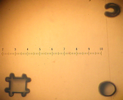
- Drilling of tiny holes through thick material (for example, 0.25 mm holes through 3-mm tungsten)
- Precise cutting of features and milling in thick materials, like stainless steel, ceramics, glass, polymers, PCB, organic capsules, micro- and nano-structured plates. Cost effective replacement of electrical discharge machining.
- Slicing and dicing of crystals with thickness up to 3 mm and micron precision.
- Imaging in fine machining with a sub-micron features, in particular marking and selected surface cleaning.
- LED cutting and slicing.
- Transparent materiel modification, high density 3D storage, hologram recording.
- Research of laser induced fluorescence and two photon ionization, single and two photon LIBS, time resolved laser, Raman and CARS spectroscopy.
- Basic research (white light excitation, Optical Parametrical Amplification with 213 nm pumping, high harmonics generation, free electron laser seeding, combustion studies, two photon polymerization).
We encourage universities and research personnel to book appointments for the services listed above in advance.
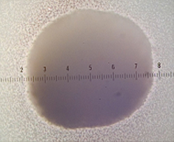
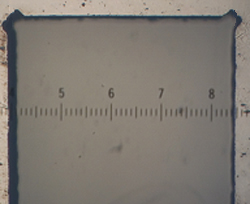
Several examples of laser processing are presented in pictures below:
Laser processing of thick material

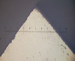

Cutting 30 microns thick diamond plate with picosecond laser